


At this year’s World Artificial Intelligence Conference in Shanghai, a startup called Dongfang Suanxin, or DFSX, set up its booth directly across from Huawei. The positioning was not subtle.
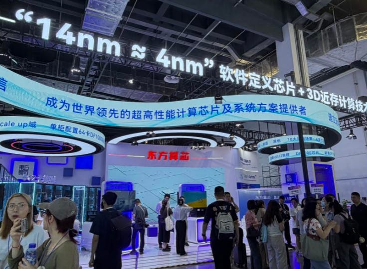
On July 13, DFSX unveiled its first chip, the DF1000, an AI accelerator that DFSX says is built entirely through a domestic supply chain using 14nm process technology. According to the company, the chip delivers 520 TFLOPS at BF16, 6.4 TB/s of memory bandwidth and 900 GB/s of scale-up interconnect bandwidth. The comparison with leading chips is narrower than it first appears: DFSX says the DF1000 can approach some 4nm-class products in selected inference workloads, while acknowledging that it still trails in training. The company says the DF2000 will close that gap.
That claim sounds improbable. On conventional measures, a 14nm accelerator should carry a substantial disadvantage in transistor density, power efficiency and peak performance.
DFSX was incorporated in 2024, but the research program behind it is not new. The company has grown to more than 500 employees. Its chairman and CEO is Wei Shaojun, a tenured professor at Tsinghua University, a member of China’s National Integrated Circuit Industry Development Advisory Committee, and one of the country’s most prominent semiconductor researchers. His team has spent nearly 20 years at Tsinghua developing reconfigurable computing architectures. The company reached a post-money valuation of roughly Rmb 12.3bn ($1.8bn) by late April 2026, with investors including the National AI Industry Fund, Hillhouse Capital, Yunfeng Capital, and funds affiliated with Meituan (China’s largest on-demand services platform), Xiaomi (consumer electronics), JD.com (e-commerce), and Didi (ride-hailing).
The investor roster signals something beyond the usual chip-startup calculus. State capital suggests policy alignment. The internet giants’ participation reads as a hedge against single-supplier dependence on Huawei, which is the most widely deployed domestic option in China’s high-end AI compute market. If DFSX delivers, these investors gain an alternative. If it does not, the write-off is likely manageable for internet companies whose balance sheets can absorb venture-scale losses.
The question DFSX raises extends beyond one company’s product launch. One premise behind US technology controls is that restricting China’s access to leading-edge fabrication and advanced memory constrains the performance of its AI systems. DFSX is testing one part of that premise: how much architecture can compensate for a mature process node.
The cost curve behind the claim
The standard narrative frames China’s use of mature process nodes as a concession. Companies that cannot access TSMC’s 4nm or 3nm fabrication settle for 14nm because they have no choice. This reading treats 14nm as a constraint to be endured.
Wei Shaojun’s own academic work suggests a different framing. In a 2019 paper, Wei estimated that developing a chip at the 14nm node could require $150m to $200m in total development spending, with sales of more than 30m units needed to amortize that cost. Cloud AI accelerators rarely reach consumer-chip volumes. The relevance for DFSX is that a reconfigurable design may spread its development cost across more workloads than a narrowly specialized chip. Whether that flexibility is sufficient to offset smaller unit volumes remains unknown. A subsequent 2020 paper in Scientia Sinica Informationis, a peer-reviewed journal of the Chinese Academy of Sciences, co-authored with 3 Tsinghua colleagues, argued that after 28nm, successive process nodes were becoming much less effective at reducing the cost per transistor, while development costs continued to rise with transistor counts.
This is not a Chinese discovery. The US Defense Advanced Research Projects Agency established its Electronics Resurgence Initiative in the late 2010s with “software-defined hardware” as a core research objective. Wei’s research program at Tsinghua had been pursuing a similar direction since 2006.
The implication is that DFSX’s choice of 14nm may reflect architectural economics as much as geopolitical necessity. If a chip can compensate for lower transistor density through smarter data movement and reconfigurable logic, mature-node fabrication may lower one part of the cost equation. But DFSX has not disclosed whether savings on logic manufacturing outweigh the cost and yield risks of 3D memory integration. The economics remain a hypothesis, not a demonstrated advantage. For certain workloads, the gap between what a chip can theoretically compute and what it usefully deliversmay narrow when architecture, not fabrication, becomes the optimization target.
The economics explain why 14nm is not irrational. They do not explain how a chip built on it could approach 4nm-class products in selected inference workloads. That depends on the combination of reconfigurable compute and 3D near-memory integration, and on whether the resulting system can survive the transition from research to production.
If the idea that Moore’s Law economics, not just export controls, are pushing Chinese chipmakers toward mature-node architecture is new to you, this is a preview of what Hello China Tech does three times a week: reading China’s AI, chip, robotics, and EV sectors from primary sources most English coverage never touches. Subscribe free to get every new analysis as it publishes.